- Research Support
- Research Resources
- Research Portal
- Office of Sponsored Projects
- College Research Administrators
- 15/5-Day Rule
- Contracts & Industrial Agreements
- Expenditure FAQs
- Lab Archives
- Research Resources
- Forms, Policies, Guidelines
- Training & Development Opportunities
- Business Service Center (BSC)
- Institutional Policies
- Institutional Datasheet
- Compliance & Integrity
- About Compliance & Integrity
- COI Disclosure
- Office of Research Security
- Export Control
- Guidance
- Hazardous Materials Management
- Human Subjects Research (IRB)
- Institutional Animal Care Program (IACUC)
- Laboratory Animal Resources Center (LARC)
- Laboratory Safety Division
- NIH Data Management
- Research Integrity Guidelines
- Research Misconduct
- Responsible Conduct of Research
- Safety Committees
- Visiting Scholars
- Collaborate & Partner
- News & Events
- About Us
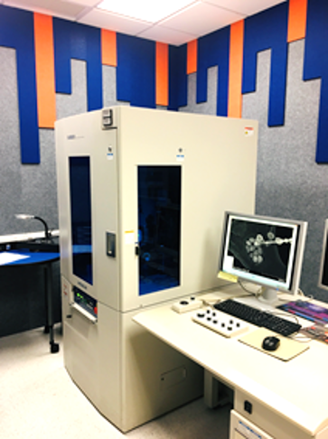
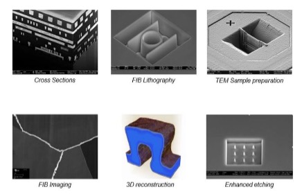
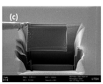
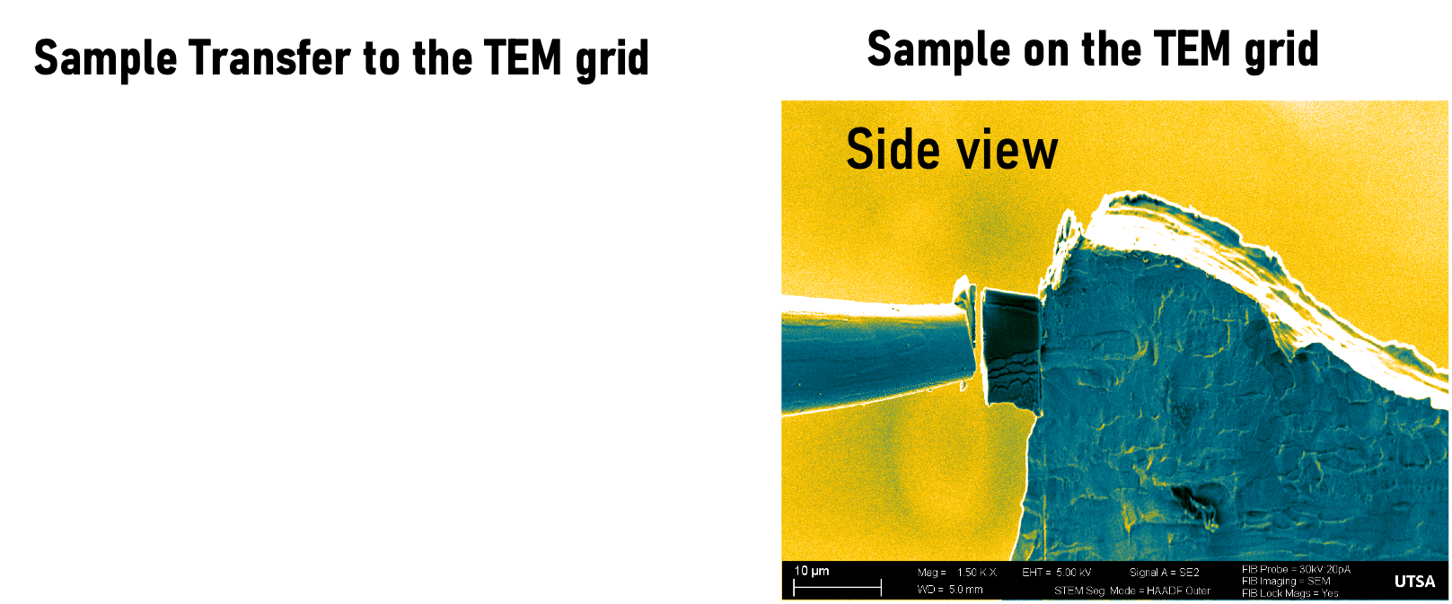
Instrumentation

Information: 210-458-4011